The Serge VCS
How it works
The following article is a slight re-working of a text that has been available on the author’s website for some years, prepared by the author for its publication in eContact! 17.4 — Analogue and Modular Synthesis: Resurgence and Evolution.
The Serge VCS (voltage-controlled slope) can perform a surprising number of tasks given that it is ostensibly a single circuit. Functions include: envelope generation (of linear, exponential or logarithmic shape); low-frequency oscillation (reaching into the audio range); voltage following, with slew-limiting; and a few other minor functions. It is a licensed adaptation of the Serge DTG/DUSG circuit (Dual Transient Generator/Dual Universal Slope Generator), which dates back to the early 1970s — the VCS has elements in common with that circuit, but it also incorporates a number of additional features. A detailed technical explanation will show how some of the more interesting aspects of the circuit work.
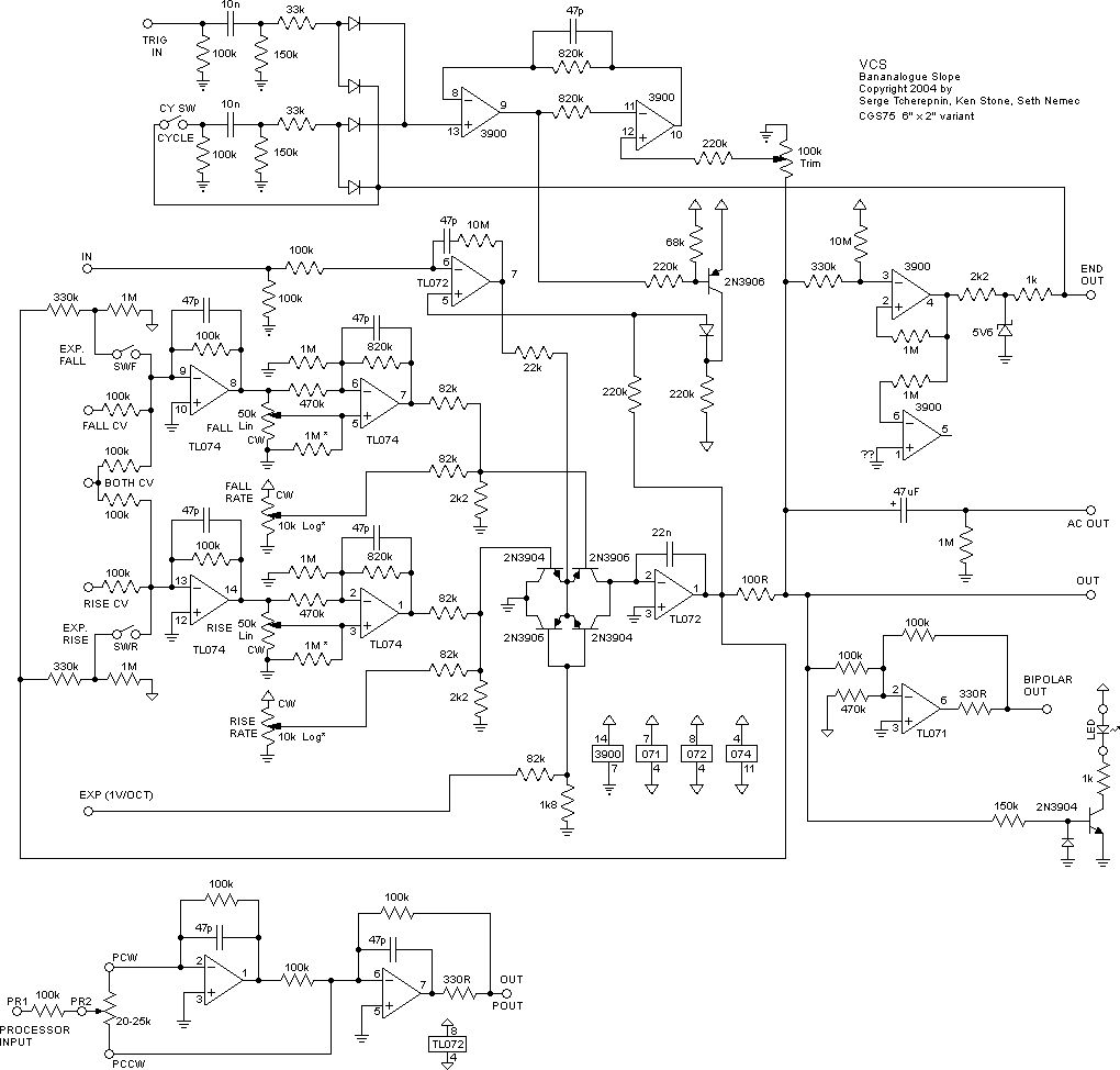
The schematic we will be working with is shown in Figure 1, which is an early embodiment of the Cat Girl Synth CGS75 / Bananalogue Serge VCS module. 1[1. The full description of the CGS75 is found on the CatGirl Synth website under the “Modules” tab. The Bananalogue module is (going to be available) through Big City Music.] Apart from the CGS75 and Bananalogue versions, in recent years other licensed versions of the Serge VCS have appeared, notably those of Doepfer (A-171-2) and Elby Designs; it is also known that the core of the circuit forms the basis for the Makenoise Maths module.
A certain level of electronics knowledge is unavoidably required of the reader. The schematic considered does not contain any component references, so amplifier sections are referred to using the pins concerned in a fairly obvious way (“LM3900 8/9/13”, and individual pins as, for example, “LM3900.9”) and resistors and capacitors are referred to via their value, but it should be clear from the context being discussed which one is meant. 2[2. Figure 1 is not the most recent schematic that appears at the CGS website — that contains a few suggested component value changes, and so the slightly older version is used for clarity purposes.]
Logic / Envelope Phase Switching

The circuit uses LM3900 current-differencing amplifiers (CDAs, also frequently referred to as “Norton amplifiers”) to implement the logic that controls the various phases during envelope generation. Compared to normal operational amplifiers (op-amps), these have a certain “inelegance” in their use 3[3. Texas Instruments still manufacture LM3900 chips. The LM3900 product page and the actual LM3900 datasheet (PDF) are available from the TI website. Presumably National Semiconductor were the originators of the chip, but as National, it had long been out of production. National were bought by TI some years ago but the original National data sheet can still be found on the TI website (PDF), and the large and very useful application note, AN-72, is also still available on the TI website (PDF). On Semiconductor’s equivalent, the Motorola MC3401, is also long since out of production, but the datasheet can be found in several places on the web, for example on datasheetarchive.com (PDF).], and they certainly make frequent appearances in Serge circuits. In the context of the current circuit their use is comparatively simple, so we start with them. 4[4. Negative feedback configurations for op-amps are easy because the feedback forces the input voltages to be the same; if negative feedback is applied to a CDA, then it does its level best to keep the currents into the inputs the same. In the absence of negative feedback, the output goes with the biggest input current: more current at the positive input, the output is high; more current into the negative input, the output is low.]
Figure 2 shows an envelope and associated logic signals. 5[5. Note that in this, and all the other scope shots, the vertical scales may be different from trace to trace!] Considering the LM3900 amplifiers 8/9/13 and 10/11/12 as a pair, the default with no trigger and the envelope low is pin 10 (orange) high (i.e. somewhat below the positive rail), which feeds current into negative input pin 8, which with no trigger/no current into pin 13, the output pin 9 (green) is low (a little above ground). On a trigger input, a pulse of current (larger than that into the negative input) into positive input pin 13 switches output 9 high; with no envelope/little current into positive input pin 12, and now lots of current into negative input pin 11, output pin 10 (orange) goes low (and note that this is unable to impact the state of pin 9, via pin 8). As the envelope climbs to its peak, the current at positive input pin 12 will exceed that into negative input pin 11, and so output 10 switches high, in turn causing output 9 to go low, back to its original state, awaiting another trigger (the exact switch-over point depends on the trimpot setting — a 6 V envelope seems typical). Thus pin 9 (green) designates “attack”, and pin 10 (orange) is “not attack”.
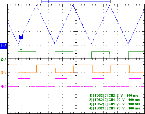
The bottom trace shown in Figure 2 (mauve) is the “end out” signal, but note this is literally pin 4 of the LM3900 being probed, so it is bigger than the 5 V or so output from the module, due to the zener diode. Its default state is high: this feeds about 10 µA back to the positive input pin 2, which, being more than that into the negative input pin 3 (about 1 µA), ensures the output stays high. When the envelope (the “out” signal) climbs above about 3 V, 10 µA or more is delivered to the negative input pin 3 (via the 330 kΩ), and this will switch the output low; the output will remain there whilst there is sufficient current into pin 3. Once the envelope falls back to near ground, all the current into pin 3 is “robbed” by the 330 kΩ resistor, and the output will flip high again — hence the “end out” signal.
Figure 3 shows the same signals when the circuit is switched into “cycle” mode, i.e. it acts as an LFO. The cycling is simply achieved by feeding the “end out” signal back as a trigger, so when end out goes high at the end of the cycle, the whole thing triggers off again for another cycle, ad infinitum.
Envelope Generation / Slew-limiting
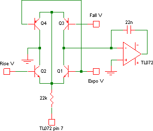
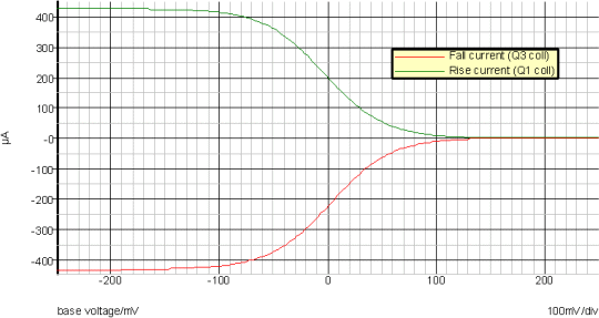
At the heart of the circuit is a simple inverting integrator, formed from section 1/2/3 of the TL072, with a 22 nF capacitor as the negative feedback loop. Feeding this is a complicated-looking arrangement of four transistors — a pair of NPNs and a pair of PNPs. If these are re-drawn (Fig. 4), it is much clearer that the transistors are merely acting as a pair of differential pairs. The tails of both pairs are wired through the 22 kΩ to output pin 7 of section 5/6/7. If, say, pin 7 is negative, then the NPN pair is on, and the PNP pair will be off, Q2 will draw current from the ground at its collector, and Q1 will draw current from the op-amp virtual ground at pin 2, so that the 22 nF charges and the output pin 1 will rise at a rate depending on the share of current between Q1 and Q2 collectors, which in turn depends on the differential voltage across their bases (“Rise V” and “Expo V”). If we plot the Q1 and Q3 collector currents, we get the familiar “tanh”-shaped curves we expect of differential pairs (Fig. 5) — this is simulation output: sweeping “Fall V” and “Rise V”; pin 7 ±10 V resp.; “Expo V” grounded.
If pin 7 is positive, then the PNP pair will be on and the NPN pair off, and now current flows in the opposite direction into the virtual ground, and the charged capacitor will now discharge, causing the output voltage to fall, at a rate this time dependent on the voltage across Q3 and Q4 bases (“Fall V” and “Expo V”). If all voltages into the transistors are held constant, the current into/out of the integrator is constant, and so the output voltage rises and falls linearly, which is what happens when we are slew-limiting or generating linear envelopes. When the rise and fall pots are pulled, this allows the pin 1 output voltage to impact the voltages at the bases (“Rise V” and “Fall V” above), hence allowing for exponential- or logarithmic-shaped envelope segments.
When generating an envelope (and not “following”), section 5/6/7 acts as a basic comparator (as the 47 pF acts as an open-circuit — more on this below) [Fig. 6]. The envelope generation operation is thus: a trigger in makes LM3900.9 go high, as described above; the PNP connected to LM3900.9 via the 220 kΩ/68 kΩ is thus turned off, so TL072.5 is pulled to -6 V or so by the two 220 kΩs on TL072.1; TL072.7 will saturate near the negative rail, so we are in the “attack” (rise) phase, the NPN pair is turned on, and output pin TL072.1 rises; TL072.5 “tracks” the envelope with an offset — it is negative and increasing; when the envelope gets to 6 V, LM3900.10 flips to high (again as above) and LM3900.9 goes low; the PNP turns on, making the diode between the 220 kΩs reverse-biased, so now TL072.5 positive input tracks the envelope exactly, which being positive, ensures the output pin TL072.7 goes to nearly the positive rail (we are assuming there is no signal at “in”), which turns the NPN pair off, the PNP pair on, and so we go to “not attack” (fall, or decay) phase, and the envelope falls. Finally, when it has fallen far enough, “end out” goes high, marking the end of the whole cycle. (Note the considerable “indecision”/oscillation at pin 7 when it has no “definite” value, as it does during the envelope cycle!)
Voltage Follower / Slew-limiter
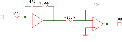
To see how the circuit functions as a voltage follower, let’s simplify things a little: from above we know that when we are in “not attack”, LM3900 pin 9 is low, the PNP is on, the diode between the 220 kΩs is reverse-biased, and so TL072.5 is only connected to TL072.1 via the 220 kΩ resistor; the op-amp has negligible input bias current, so we can ignore the 220 kΩ and show pins 5 and 1 connected directly; the two differential pairs setup complicates things too, so let’s replace all of that with a simple resistor, Requiv, say. The circuit we now have to deal with is shown in Figure 7.
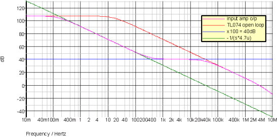
The operation of the inverting integrator (right side of Fig. 7) formed from TL072 1/2/3 is still clear, so now we concentrate on the action of the first amplifier (which, as we mentioned above, sometimes acts as a basic comparator). For the purposes of this analysis, let’s assume the non-inverting input (pin 5) is grounded. Then at higher frequencies, the reactance of the 47 pF capacitor is negligible when compared to the 10 MΩ resistor, and so the whole simply looks like a x100 inverting amplifier (i.e. we get 40 dB of gain). At lower frequencies, it is the other way round — the capacitive reactance dominates, so this looks like an inverting integrator with the 0 dB frequency given by 1/(2π×47e–12×100e3) = 33.8 kHz. The integrator’s “1/s” line comes back up from this point at 20 dB/decade, meeting the 40 dB line at 338 Hz, and thus for frequencies above about 300 Hz the amplifier gives a gain of 40 dB, and for lower frequencies, the gain is even more. The frequency response in Figure 8 shows the overall amplifier response, along with these two other curves, and the TL072/074 open-loop response (which ultimately limits the available gain).
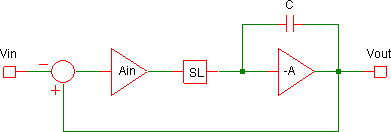
Thus for DC signals the maximum (open-loop) gain of the op-amp is available, and hence the assertion that for such signals it acts like a simple comparator is seen to be valid. Replacing this amplifier with a simple gain block “Ain” results in an arrangement that looks like Figure 9, where now block “SL” is responsible for the slew-limiting effect. 6[6. It is not too difficult to do a slightly more rigorous analysis that shows that this gain approximation still holds even when the non-inverting input is no longer held at ground.] Setting the feedback loop aside for the moment, this bears more than a passing resemblance to the simple integrator / one-pole model often used for a standard op-amp, shown in Figure 10. 7[7. For more on the topic, see Sedra 1982, p. 837. For a slightly more complex view, see Schaumann 2001, p. 19, or Franco 2002, p. 259.]
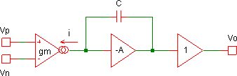
The transconductance input stage, gm (a differential pair or the like), feeds an inverting integrator; an inherent characteristic of the gm stage — the maximum current it can deliver — imposes the slew-rate limit on the op-amp by preventing the integrator output voltage from changing as fast as it would like. The VCS circuit replicates this action, only in this case the slew-rate limit is deliberately imposed by the two differential pairs that constitute the SL block, limiting the current feeding the main integrator (and thus the slew-limiting is determined by the voltages controlling the differential pairs). It is not too difficult to show that this arrangement does indeed give a voltage-follower/unity gain. From the diagramme shown in Figure 9, the output of the Ain block is Ain(Vout-Vin) and thus, taking the integrator as -1/(τs):
Vout = -Ain(Vout-Vin)/(τs)
which is easily re-arranged to give:
Vout/Vin=Ain/(τs+Ain) = 1/(τs/Ain+1) ≈ 1
which is the unity gain we seek, as long as 1>>τ/ Ain, i.e. Ain is big and τ is small (τ is the effective time-constant of the integrator, dependent on the 22 nF capacitor and the slew-limit current from the differential pairs). 8[8. Mention of phase and stability considerations has been avoided here — suffice it to say that it does just about manage to hang together. Of greatest concern is the phase from the output of the input amplifier (pin 7) back round to its non-inverting input (pin 5): the signal travels through the main (inverting) integrator, which thus has a phase lead of 90°, giving +90° at pin 5; this in turn is halfway between positive feedback (0°) and negative feedback (180°), but as it doesn’t seem to be associated with any of the usual detrimental qualities of positive feedback, it is regarded here as being negative feedback. The input amplifier itself also has large phase changes between working as an integrator at low frequencies, to a straight inverting amplifier higher up.]
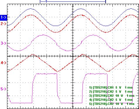
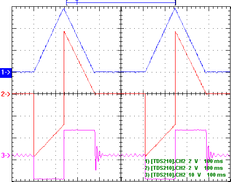
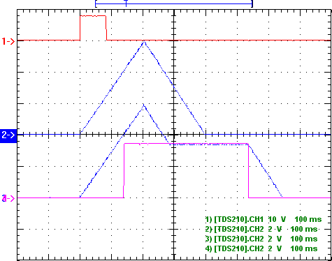
Figure 11 shows voltage-following scope traces when slew-limiting and not slew-limiting. The top pair of red and blue traces shows that the output is following the input, with the slew-rate set to max, i.e. both rise and fall pots fully counter-clockwise. Trace 3 (mauve) is the corresponding pin 7 signal for this case — it is actually the negation of the derivative of the input. This isn’t difficult to show analytically, but as the output of the main integrator is the same as the input signal, the input to the integrator must be the derivative of the input signal (plus the sign inversion). The bottom set of traces is when the slew-limiting is just coming into effect, by turning the rise and fall pots clockwise: trace 4 (red) is the resultant slew-limited, hence triangular, output signal; trace 5 (mauve) is pin 7, which is now saturating near the supply rails. (If a triangle wave is input, and which isn’t slew-limited, pin 7 will also be a square wave, the amplitude of which will be proportional to the rising and falling slopes of the wave.)
Adding Sustain to an Envelope
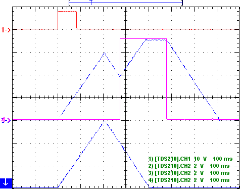
This is achieved by the simple expedient of inputting a pulse of the requisite amplitude into the input whilst an envelope has been triggered — this will cause the envelope to follow the pulse at the appropriate point (Fig. 12). Note that even though the sustain pulse starts during attack, it is ignored, because the LM3900.9 is low, the PNP is on, and the diode between the 220 kΩs “interrupts” the signal from TL072.1 to TL072.5. Once in “not attack”, the envelope will slew down until it reaches the sustain pulse, and then follow it; at the end of the pulse the envelope again slews down normally. Figure 13 shows what happens when the pulse is actually greater than the envelope 6V-point for switching from attack to not attack — it will slew up to the pulse amplitude, and then follow it, again slewing to ground when the pulse finishes.
Bibliography
Franco, Sergio. Design with Operational Amplifiers and Analog Integrated Circuits. 3rd Edition. New York: McGraw-Hill, 2002.
Schaumann, Rolf and Mac E. van Valkenburg. Design of Analog Filters. New York: Oxford University Press, 2001.
Sedra, Adel and Kenneth Smith. Microelectronic Circuits. 4th Edition. New York: Oxford University Press, 1982.
Social top